
Hacking a Coin Acceptor
Coin acceptors like LINK are relativiely cheap and can interface with a microcontroller but have several issues that this exercise attempts to overcome. Most significantly they are slow when using the pulse output to communicate with your microcontroller.
Firstly there is a signifacant delay between dropping the coin in and getting output data to start. By the time data gets set the coin is alreadt through the device an in the coin box. Normally not an issue but if you wanted to manually control the solenoid on the device this is WAY too late. A user that inserts coins "too fast" can also cause issues because the pulses simply get chained together. There is a possibility to game the device in this way if it's not set up correctly.
Another data output is from the debugging port and this is very fast. The problem is that it's undocumented and interpretation of the data is problematic.
Removing the PCB though provides another access point to fast data aquisition. Observation of the LEDs and the 7 segment display reveals the coin data appears very quickly. If these data are intercepted and output to the microprocessor we can have a fast and accurate data source. Two pads need to be desoldered, the connections to the coil at the top of the PCB.
The 7 segment display is driven with a 74HC164 serial to parallel chip. We can intercept the serial data going to the chip and read his with out microcontroller. The pins we are interested are 1+2 which has the data, and pin 8 which is clock data. Tapping this off we have SPI data that an AtTiny can directly read and interpret what the 7 segment display shows.
The debugging connector, on my prticular con acceptor, has six pins, not all of which are connected. The pins opposite the GND pin have no connections and we can use these by connecting them to the data and clock lines.
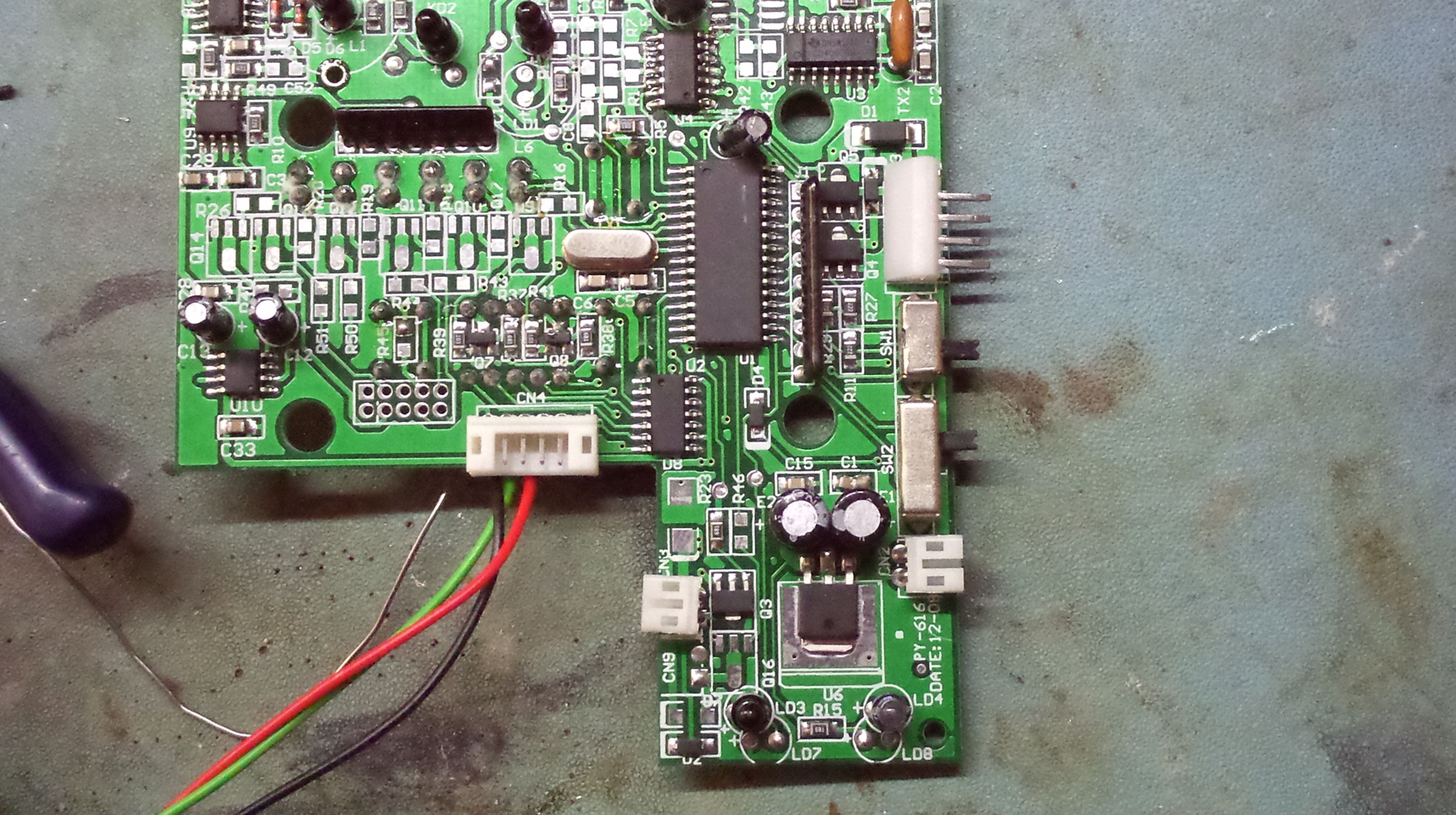
In the, rather large, image above the tracks we want to connect to are the two that run vertcally from the larger processor chip to the smaller 74HC164. Link these to the two unused pins on the RHS of the six way connector. Top one (on the processor) is data, the adjacent lower one is clock. Apologies for the image size but it shows details. Also not the missing components that can connect the LEDs and the empty mystery connector. Not yet sure if these are inuts or outputs.
Decoding the data has already been done by https://github.com/fablab-bayreuth/coinspi Look into the main.c file for the decoding. Note that the data are sent three times to the display. Take care to ignore the repeats.
More to come concerning coding an AVR AtTiny84. Warm up GCC and your favourite text editor.
Relevent links:
http://blog.deconinck.info/post/2017/02/25/CH923/CH926/CH928-coin-acceptor-features-and-caveats
https://github.com/fablab-bayreuth/coinspi/blob/master/main.c
Last changed: 21. April, 2021 at 11:03
Back to OverviewComments
Add Comment